


Description
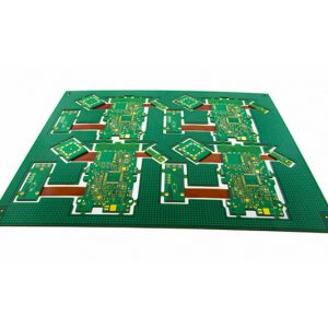
HDI Printed Circuit Boards
HDI boards, one of the fastest growing technologies in PCBs, are now available at FCC GROUP. HDI Boards contain blind and/or buried vias and often contain microvias of .006 or less in diameter. They have a higher circuitry density than traditional circuit boards.
There are 6 different types of HDI boards, through vias from surface to surface, with buried vias and through vias, two or more HDI layer with through vias, passive substrate with no electrical connection, coreless construction using layer pairs and alternate constructions of coreless constructions using layer pairs.
Consumer Driven Technology
The via-in-pad process supports more technology on fewer layers, proving that bigger is not always better. Since the late 1980’s we have seen video cameras using cartridges the size of a novel, shrink to fit in the palm of your hand. Mobile computing and working from home pushed technology further to make computers faster and lighter, allowing the consumer to work remotely from anywhere.
HDI Technology is the leading reason for these transformations. Products do more, weigh less and are physically smaller. Specialty equipment, mini-components and thinner materials have allowed for electronics to shrink in size while expanding technology, quality and speed.
Key HDI Benefits
As consumer demands change, so must technology. By using HDI technology, designers now have the option to place more components on both sides of the raw PCB. Multiple via processes, including via in pad and blind via technology, allow designers more PCB real estate to place components that are smaller even closer together. Decreased component size and pitch allow for more I/O in smaller geometries. This means faster transmission of signals and a significant reduction in signal loss and crossing delays.
Cost Effective HDI
While some consumer products shrink down in size, quality remains the most important factor for the consumer second to price. Using HDI technology during design, it is possible to reduce an 8 layer through-hole PCB to a 4 layer HDI microvia technology packed PCB. The wiring capabilities of a well-designed HDI 4 layer PCB can achieve the same or better functions as that of a standard 8 layer PCB.
Although the microvia process increases the cost of the HDI PCB, the proper design and reduction in layer count reduces cost in material square inches and layer count more significantly.
Building Non-Conventional HDI Boards
Successful manufacturing of HDI PCBs requires special equipment and processes such as laser drills, plugging, laser direct imaging and sequential lamination cycles. HDI boards have thinner lines, tighter spacing and tighter annular ring, and use thinner specialty materials. In order to successfully produce this type of board, it requires additional time and a significant investment in manufacturing processes and equipment.
Laser Drill Technology
Drilling the smallest of micro-vias allows for more technology on the board’s surface. Using a beam of light 20 microns (1 Mil) in diameter, this high influence beam can cut through metal and glass creating the tiny via hole. New products exist such as uniform glass materials that are a low loss laminate and low dielectric constant. These materials have higher heat resistance for lead free assembly and allow for the smaller holes to be used.
Lamination & Materials For HDI Boards
Advanced multilayer technology allows for designers to sequentially add additional pairs of layers to form a multilayer PCB. The use of a laser drill to produce holes in the internal layers allows for plating, imaging and etching prior to pressing. This added process is known as sequential build up. SBU fabrication uses solid filled vias allowing for better thermal management, a stronger inter connect and increasing the board’s reliability.
EXTREME COPPER PRINTED CIRCUIT BOARDS
The special requirements for the design of heavy copper printed circuit boards, EXTREME copper printed circuit boards and PowerLink technology and other forms of component mounting and interconnecting structures incorporating copper weights ≥ 3oz/ft2. Some sections of this standard are guidelines ONLY, and are noted as such.
The requirements contained in this standard are intended to establish design recommendations that are to be used in conjunction with the design principles laid out in IPC-2221, IPC-2222.
This standard’s intended use is by printed circuit board designers who incorporate copper weights ≥ 3oz/ft2 into their products.
General Design Considerations
The general parameters to be considered before and during the design of any printed circuit board, but focuses on boards incorporating copper weights ≥ 3oz/ft2. The following parameters can and will have a major impact on reliability and performance of the end product. FCC GROUP believes the parameters listed in this section are a MINIMUM to be considered. A comprehensive listing of all parameters and their design/performance tradeoffs is shown in IPC-2221.
End-Product Requirements
The end product requirements must be known before design start-up. Servicing and maintenance of the end product can directly influence conductor routing, part placement, board size, markings, coatings and final finish.
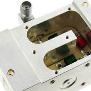
Microwave & RF Circuit Boards
MICROWAVE & RF PRINTED CIRCUIT BOARDS
In order to meet increasing demands for Microwave & RF Printed Circuit Boards for our customers all around the world, we have increased our investment over the last few years so that we have become a world class manufacturer of PCB’s using high frequency laminates.
These applications typically require laminates with specialized electrical, thermal, mechanical, or other performance characteristics that exceed those of traditional standard FR-4 materials. With our many years of experience with PTFE-based microwave laminate, we understand the high reliability and tight tolerance requirements of most applications.
Our experience allows us to provide our customers with most comprehensive service in circuit board production for these products as we have invested in.
PCB Material Stock
Will all the different features of every RF PCB application, we have developed partnerships with the key material suppliers such as Rogers, Arlon, Nelco, and Taconic just to name a few. While many of the materials are very specialized, we do hold significant stock of product in our warehouse from Rogers (4003 & 4350 series) and Arlon. Not many companies are prepared to do that given the high cost of carrying inventory to be able to respond quickly.
High technology circuit boards fabricated with high frequency laminates can be difficult to design because of the sensitivity of the signals and the challenges with managing the thermal heat transfer in your application. The best high-frequency PCB materials have low thermal conductivity versus the standard FR-4 material used in standard PCBs.
RF and microwave signals are very sensitive to noise and have much tighter impedance tolerances than traditional digital circuit boards. By utilizing ground plans and using a generous bend radius on impedance controlled traces can help make the design perform in the most efficient manner.
Because wavelength of a circuit is frequency dependent and material dependent, PCB materials with higher dielectric constant (Dk) values can result in smaller PCBs as miniaturize circuit designs can be used for specific impedance and frequency ranges. Oftentimes high-Dk laminates (Dk of 6 or higher) are combined with lower cost FR-4 materials to create hybrid multilayer designs.
Understanding the coefficient of thermal expansion (CTE), dielectric constant, thermal coefficient, temperature coefficient of dielectric constant (TCDk), dissipation factor (Df) and even items like relative permittivity, and loss tangent of the PCB materials available will help the RF PCB designer create a robust design that will exceed the required expectations.
Specialized Processing Equipment
Much of the processing for Microwave/RF PCB’s can be done on standard fabrication equipment. However, the need for specialized equipment is requires for the most demanding designs. We have in house Plasma Etch equipment to ensure that the quality of the thru holes is at the highest level. Along with that we use Laser Direct Imaging (LDI) equipment versus the more traditional photo exposure tools so that we can hold very tight trace widths and front to back registration requirements.
Wide Ranging Capabilities
In addition to standard Microwave/RF PCB’s :
- Hybrid or Mixed Dielectric Boards (PTFE/FR-4 combinations)
- Metal Backed and Metal Core PCB’s
- Cavity Boards (Mechanical and Laser Drilled)
- Edge Plating
- Constellations
- Large Format PCB’s
- Blind/Buried and Laser Via’s
- Soft Gold and ENEPIG Plating
Reviews
There are no reviews yet.